english.elpais.com ·
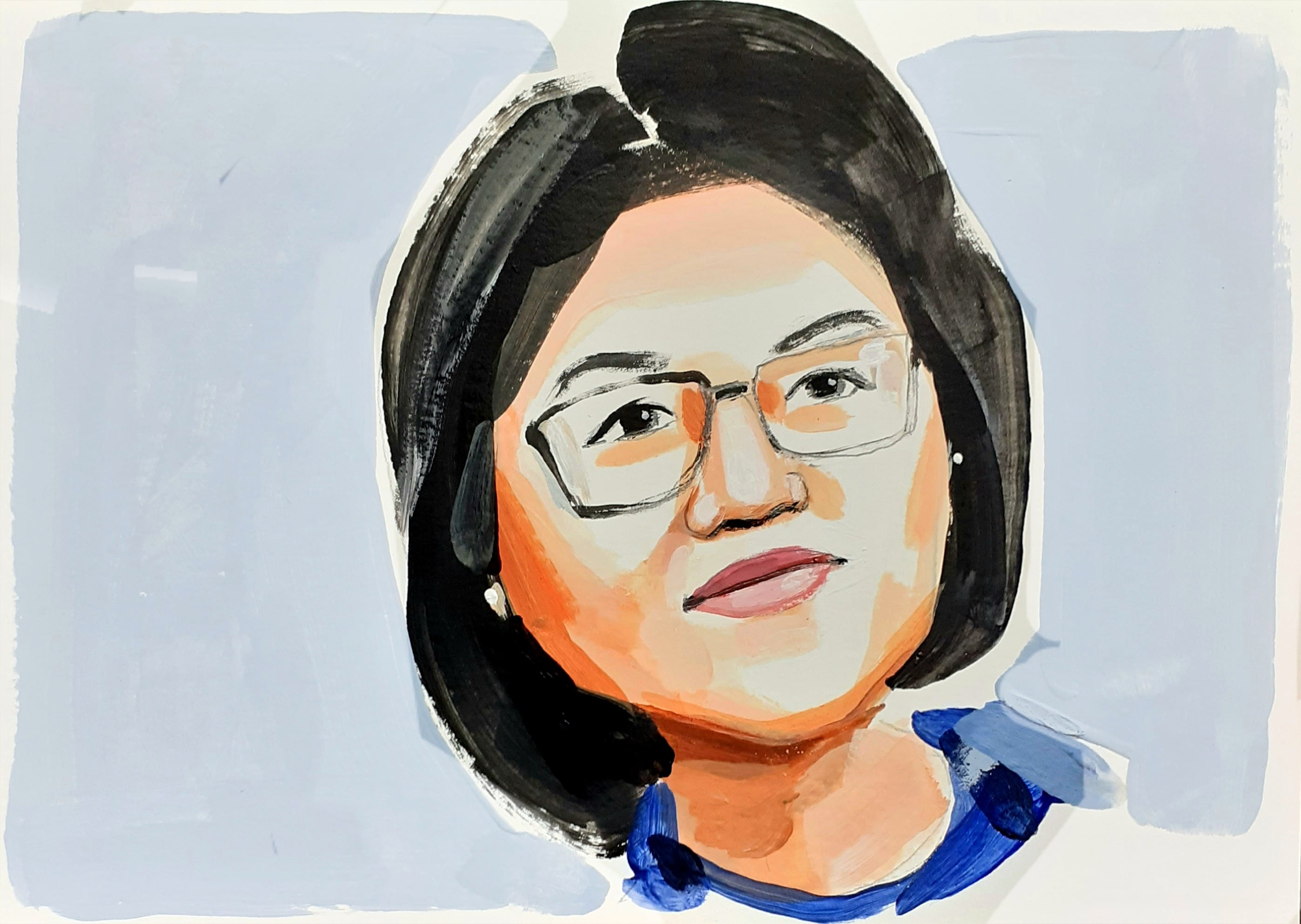
He Tingbo the Woman WHO Wants to Change the Chip Industry
News Analysis — AI Analysis
Original analysis generated by News Analysis. This is our own commentary on the story, not the publisher's article text.
Facing the limitations of Moore's Law, He Tingbo, president of Huawei’s semiconductor business, has proposed an alternative framework called the Tau scaling law. This new method suggests improving chip efficiency by reducing signal travel time rather than continuously shrinking transistor size. The technology utilizes LogicFolding to stack circuits vertically in layers, a technique that could be featured on Huawei's upcoming Kirin 2026 chip.
Key points
- Moore’s Law, which predicted doubling transistor density every two years, has reached its limits for modern computing.
- He Tingbo introduced the Tau scaling law, proposing to trade size reduction for time efficiency in chip design.
- The method involves LogicFolding, a technique that stacks circuits vertically in multiple layers rather than spreading them on a single plane.
- Huawei has reportedly mass-produced 381 chips using this new technology, with the Kirin 2026 expected to debut it.
- He Tingbo's focus on self-sufficiency and R&D is highlighted as a response to U.S. trade sanctions against Huawei.
Claims assessed
- VerifiableThe Tau scaling law proposes improving chip power and efficiency by reducing the time electrical signals take to travel between components.
- VerifiableLogicFolding is a technique that stacks circuits vertically in layers, moving away from single-plane circuit designs.
- VerifiableHuawei's Kirin 2026 chip could be the first globally to incorporate the Tau scaling technology.
- VerifiableHe Tingbo credits U.S. sanctions for forcing Huawei to achieve self-sufficiency and invest heavily in R&D.
Missing context
The article does not provide detailed technical specifications or independent validation regarding the feasibility, manufacturing yield, or long-term viability of 3D stacking (LogicFolding) compared to established industry standards like those used by TSMC. Furthermore, it only mentions Huawei's significant R&D investment in 2025 but does not detail its current financial standing relative to globa…
Topic context
The full article is on the original publisher site.
AI insight
AI-generatedHuawei's demonstration of Tau scaling boosts confidence in regional technological autonomy, positively affecting specialized EDA tools (SEMICONDUCTORS) and industrial control systems (EM_INDUSTRIALS) short-term. Main risk: The immediate positive sentiment is likely to overstate actual revenue or margin gains without confirmed contract awards or sustained global demand.
The announcement of the Tau scaling law by Huawei signals a technological pivot toward vertical stacking (LogicFolding) to maintain performance gains without relying solely on traditional transistor shrinking (Moore's Law). This is a direct response to U.S. sanctions, aiming to enhance self-sufficiency in chip design and manufacturing for advanced processors like Kirin 2026. The primary impact is on Huawei's internal cost structure and long-term market competitiveness within the EM_TECH sector.
Signals our AI researcher identified
Extracted by our AI model from this article and related public sources — not direct quotes from the publisher.
- Huawei's semiconductor business head introduced Tau scaling law (alternative to Moore's Law)
- Tau scaling involves stacking circuits vertically using LogicFolding technique
- Huawei mass-produced 381 chips using this method
- Kirin 2026 is expected to be the first chip featuring Tau scaling
- Development follows U.S. sanctions impacting Huawei's capabilities
Affected products & commodities
- Semiconductor chips
- Kirin 2026 processor
Supply-chain signals
- Advanced chip design methodology (Tau scaling)
- Vertical circuit stacking technology (LogicFolding)
Historical parallels
- Previous shifts in semiconductor manufacturing (e.g., transition from planar to FinFET) often lead to temporary supply chain bottlenecks and increased capex requirements for new fabrication nodes, but the long-term trend is sustained demand.
This analysis would be wrong if
If the market fails to see concrete evidence of new, large-scale government procurement contracts or specific foundry capacity reservation payments linked directly to Tau scaling adoption.
The shift to domestic advanced chip design solidifies China's position in critical industrial technology supply chains. The key risk is that sustained margin gains depend on confirmed large-scale government contract awards.
Sign in to see all sector verdicts, full thesis and counter-argument debate.
Sector impact at a glance
- EM_INDUSTRIALSmid
- EM_INDUSTRIALSshort
- GLOBAL_TECHshort
- SEMICONDUCTORSshort
Related stories

wral.com
B101f Africas Ebola Outbreaks Complicated by Victims WHO Prefer Traditional Healers Over Hospitals

clickorlando.com
Africas Ebola Outbreaks Complicated by Victims WHO Prefer Traditional Healers Over Hospitals

greenleft.org.au
Gaza Flotilla Participant Labor Wrong Side History

namibian.com.na
We Fear for Our Lives Deadline for Migrants to Leave South Africa Looms

thedailybeast.com